网站分类
搜索
最新留言
文章归档
友情链接
博伊西州立大学《AMT》:在激光诱导石墨烯上化学镀铜,用于柔性混合电子应用
1成果简介
柔性混合电子器件(FHE)将柔性基板与传统电子元件相结合,提高了机械稳定性,缩小了尺寸,减轻了重量。激光诱导石墨烯(LIG)为柔性器件的图案化提供了一种新方法,其特点是重量轻、柔性好、易于合成。本文,博伊西州立大学David Estrada等研究人员《ADVANCEDMATERIALS TECHNOLOGIES》期刊发表名为“Electroless Plating of Copper on Laser-Induced Graphene for Flexible Hybrid Electronic Applications”的论文,研究展示了一种利用镀铜石墨烯制造直接写入、按需柔性电子器件的新工艺。该方法将催化活性钯纳米粒子融入 LIG 结构中,实现了选择性镀铜以形成电路。这种方法省去了敏化步骤,避免了电镀中的均匀沉积难题,从而简化了工艺。
我们系统地研究了激光通量对 LIG 结构和电镀行为的影响,确定了使用7 W、450 nm 激光的最佳通量为168J cm-2。使用这种能量的样品可在 20 分钟内完全镀铜,板电阻为149.9mΩ -1,具有良好的附着力和 10 000 次弯曲周期的耐久性。在柔性聚酰亚胺基底上生产出了运算放大器,证明了这一工艺在制造低成本 FHE 方面的可行性。这项研究扩大了 LIG 的应用范围,并确定了激光能量与镀铜行为之间的关系,为将 LIG 集成到柔性电子产品中开辟了新的机遇。
2图文导读
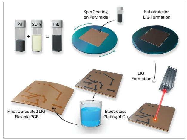
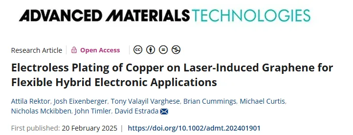
图1、创建 Cu-LIG FHE 的工艺流程。从左上角开始,顺时针向右:形成 Pd 和 SU-8 的混合物,旋涂到聚酰亚胺薄膜上并干燥,在聚酰亚胺基板上用 Pd/SU-8 油墨形成 LIG,最后,化学镀铜形成导电电路元件。
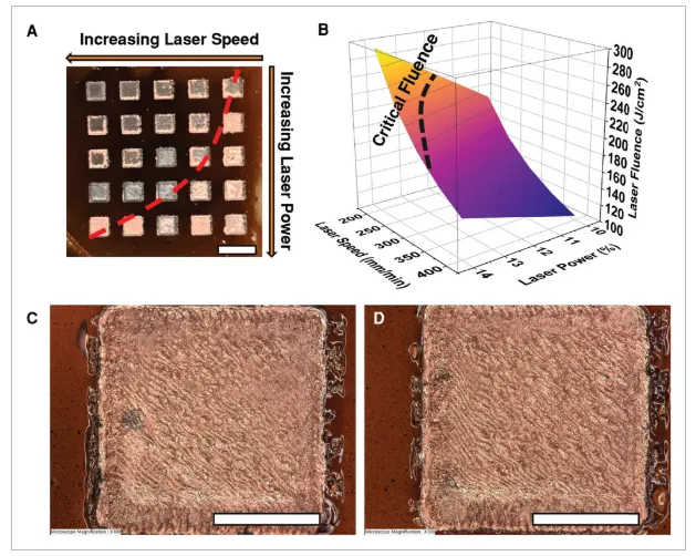
图2、A) The grid of Pd-LIG formed at various parameters, starting at 200mmmin−1and increasing in 50mmmin−1increments, with laser power at 10%/0.7W and increasing in 1%/0.7W increments, the red dashed line indicates the minimum critical fluence to result in plating, plating time is 20min and scale bar is 4mm, B) A plot of laser fluence versus laser speed and power, the red-dashed line shows the minimum critical fluence to result in copper plating, C-D) Optical microscopy of the best copper-plated samples, at 14% – 400 mmmin−1and 13% – 400 mmmin−1, respectively, scale bar is 1mm.
图3、Raman spectra collected from various combinations of laser speed and power, resulting in various fluences, A) Highlighted Raman spectra of the five different speeds tested at 14%/0.98W with their corresponding ID/IGratio, B) The full combination of 2 × 2mm LIG structures lased at the various speeds and power that were investigated, ranging from 10%/0.7W to 14%/0.98W and 200 to 400mmmin−1. The 14%/0.98W and 400mmmin−1sample is chosen as the best combination for copper plating based on subsequent plating results.
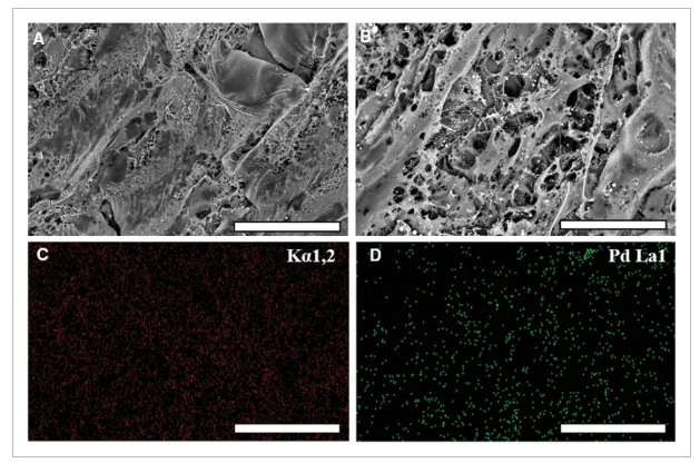
图4、A,B) SEM analysis of the Pd-incorporated LIG structure before copper-plating, at 100 and 50 µm. The high contrast particles, visible in B), are Pd NPs, C-D) EDS analysis of the SEM region from B), showing the expected carbon response in C), and homogenous integration of Pd into the LIG structure in D), scale bars are 50 µm.
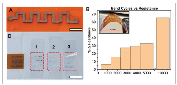
图5、A) Cu-LIG serpentine pattern lased from the Pd/SU-8/polyimide combination, scale bar is 8mm, B) Total change in resistance plotted against number of bend cycles, up to 10000, inset is the Cu-LIG loaded onto bending apparatus with a 0.87cm bend radius, and C) Adhesion testing of Cu-LIG test structures in accordance with IPC-650-2.4.1, showing copper removal occurs from structure edges.
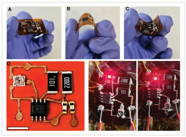
图6、The fully patterned Cu-LIG op-amp, A) in an unflexed state, B) flexed into a convex position, and C) flexed into a concave position. D) Circuit lay-out for the surface-mounted components, including resistors, LEDs, and IC op-amp. E) Demonstration of the switching behavior showing the alternating behavior of the LEDs.
3小结
这项研究提出了一种新颖而简便的方法,将铜锂基极阵(Cu-LIG)应用于 FHE 的图案化,最终制造出灵活的运算放大器。这是通过在 LIG 结构中直接加入催化活性PdNPs,以通过无电解镀铜还原铜离子来实现的。作为镀铜行为背后的驱动力,对通量进行了研究,并将其优化为168J cm-2,对应于 14%/0.98W - 400mm min-1,焦距偏移为±0mm。此外,在不同的通量点上观察到一种趋势,即最低通量阈值为147J cm-2,即可成功镀铜。在 14%/0.98 W - 400mm min-1的组合下,通过该工艺生产的铜-LIG 显示出低至 149.9 mΩ -1的薄片电阻、铜/LIG 界面的良好附着力,以及在 10,000 次弯曲循环中电阻略微增加 65%。我们的工艺采用了一台简单的业余级台式数控机床,配备了一台7W、450 nm 的可见光激光器。快速电路原型的能力与 LIG 固有的可调性相结合,产生了一种快速成型制造方法,扩大了 FHE 的生产范围,并为未来的 FHE 便捷制造提供了解决方案。
文献: