网站分类
搜索
最新留言
文章归档
友情链接
激光二极管发出深紫外光
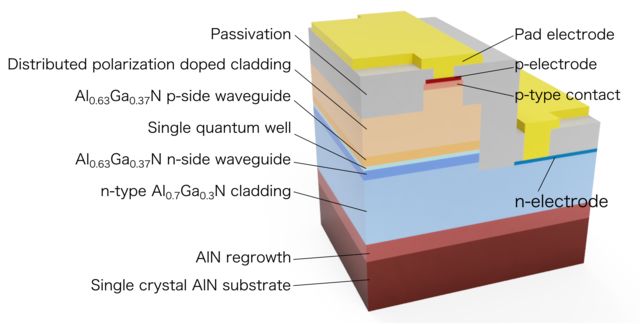
UV-C半导体激光二极管的横截面结构。
能够发射短波紫外线的激光二极管被简称为UV-C,其波长范围为200~280纳米,可用于医疗消毒、皮肤病治疗,以及气体和DNA分析。"Our laser diode emits the world's shortest lasing wavelength, at 271.8 nanometers (nm), under pulsed [electric] current injection at room temperature," says Professor Chiaki Sasaoka of Nagoya University's Center for Integrated Research of Future Electronics.
脉冲作用下,UV-C半导体激光二极管的发射特征
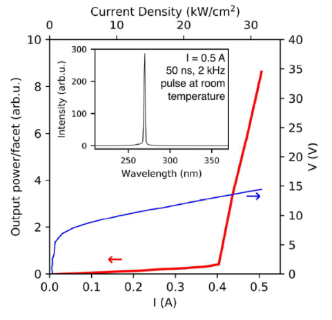
Fig. 2. (Color online) I–V and edge emission I–L characteristics of measured UV-C LD. The inset figure shows the edge emission spectrum at 0.5 A forward current.(插图显示了正向电流为0.5 A时的边缘发射光谱。)
Chiaki Sasaoka教授等开发的深紫外激光二极管克服了半导体器件研制过程中的若干问题。他们以高质量氮化铝作为激光二极管层的基底。研究人员表示,此举非常必要,因为低质量的氮化铝包含大量缺陷,会影响激光二极管活性层将电能转化为光能的效率。
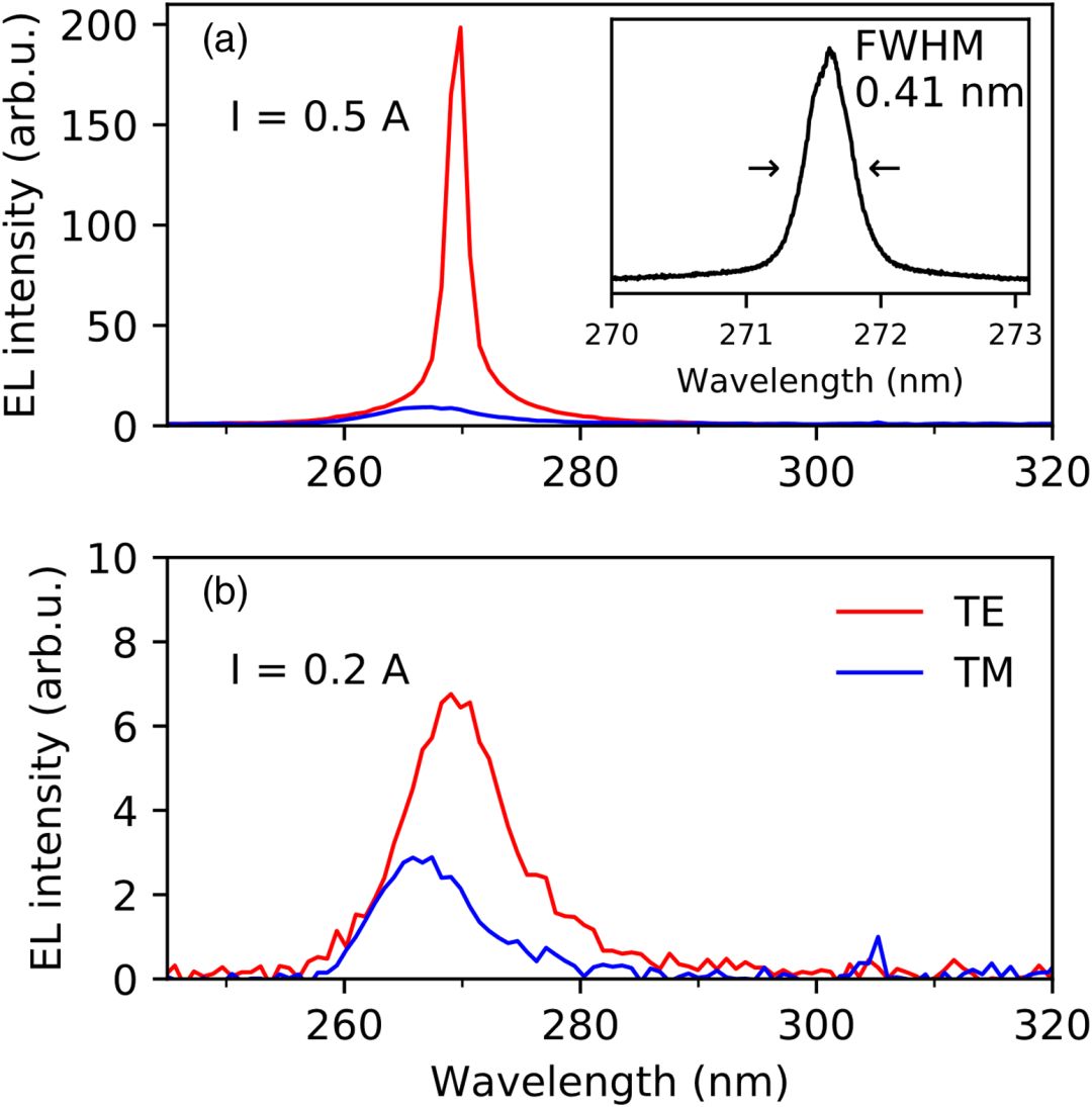
Fig. 3. (Color online) Edge emission spectra with TE and TM polarization at (a) 0.5 A and (b) 0.2 A forward current. The inset figure in (a) shows the spectrum of the TE mode at 0.5 A with the highest wavelength resolution.(在(a)0.5 A和(b)0.2 A正向电流下具有TE和TM极化的边缘发射光谱。(a)中的插图显示了在0.5 A下具有最高波长分辨率的TE模式的光谱。)
在激光二极管中,“p型”层和“n型”层被“量子阱”分隔开。当电流通过激光二极管时,p型层中的正电荷空穴和n型层中的负电荷电子会向中心集结,最终以光子的形式释放能量。研究人员对量子阱进行了设计,使它能发射出深紫外光。他们用氮化镓铝制备了p型层、n型层和覆层。覆层分别位于p型层和n型层两侧。研究人员以掺杂方式在n型层下方的覆层中加入了硅杂质,以分布极化掺杂的方式在p型层上方的覆层中加入了其它杂质。p型层一侧的覆层设计为底部最高,逐渐向顶部递减。研究人员认为,铝梯度可增强正电空穴的流动。最后,研究人员制造了以镁掺杂氮化镓铝为主的表面接触层。实验中,研究人员发现,脉冲电流只需满足13.8伏特的低工作电压即可使偏振掺杂的p型层发射出迄今为止最短波长的紫外线。In laser diodes, a 'p-type' and 'n-type' layer are separated by a 'quantum well'. When an electric current is passed through a laser diode, positively charged holes in the p-type layer and negatively charged electrons in the n-type layer flow towards the center to combine, releasing energy in the form of light particles called photons.
The researchers designed the quantum well so that it would emit deep UV light. The p- and n-type layers were made from aluminium gallium nitride (AlGaN). Cladding layers, also made from AlGaN, were placed on either side of the p- and n-type layers. The cladding below the n-type layer included silicon impurities, a process called doping. Doping is used as a technique to modify a material's properties. The cladding above the p-type layer underwent distributed polarization doping, which dopes the layer without adding impurities. The aluminium content in the p-side cladding was designed so that it was highest at the bottom, decreasing towards the top. The researchers believe this aluminium gradient enhances the flow of positively charged holes. A top contact layer was finally added that was made from p-type AlGaN doped with magnesium.
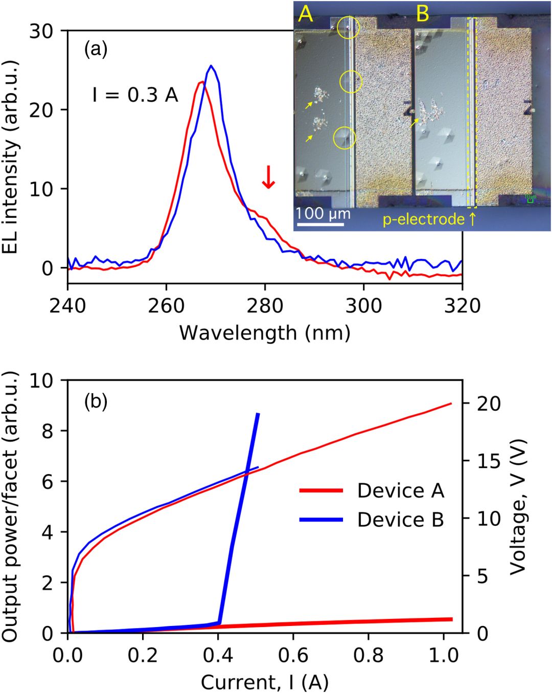
Fig. 4. (Color online) Comparison of the (a) edge emission spectra at 0.3 A forward current and (b) I–V, I–L characteristic of two adjacent devices; (A): with, and (B): without p-electrode stepping on HPHs. The inset picture in (a) shows the optical microscope image of both devices. Circles indicate HPHs that overlapped with the p-electrode. Arrows indicate probe scratches.
目前,Sasaoka教授团队正在与旭化成公司进行联合开发,以实现室温条件下连续深紫外激光的发射,进而开发出UV-C半导体激光产品。

日本名古屋大学

原文链接:1.
论文原文免费下载网址:
LETTER,A 271.8 nm deep-ultraviolet laser diode for room temperature operation,Ziyi Zhang1,2,Maki Kushimoto3,Tadayoshi Sakai3,Naoharu Sugiyama2,Leo J. Schowalter2,4,Chiaki Sasaoka2andHiroshi Amano2
Published 7 November 2019•© 2019 The Japan Society of Applied Physics
Applied Physics Express,Volume 12,Number 12,Spotlights 2019
来自:激光二极管发出深紫外光,科界SciMall,来源科技工作者之家—科界App

Over
江苏省激光产业技术创新战略联盟会议预告